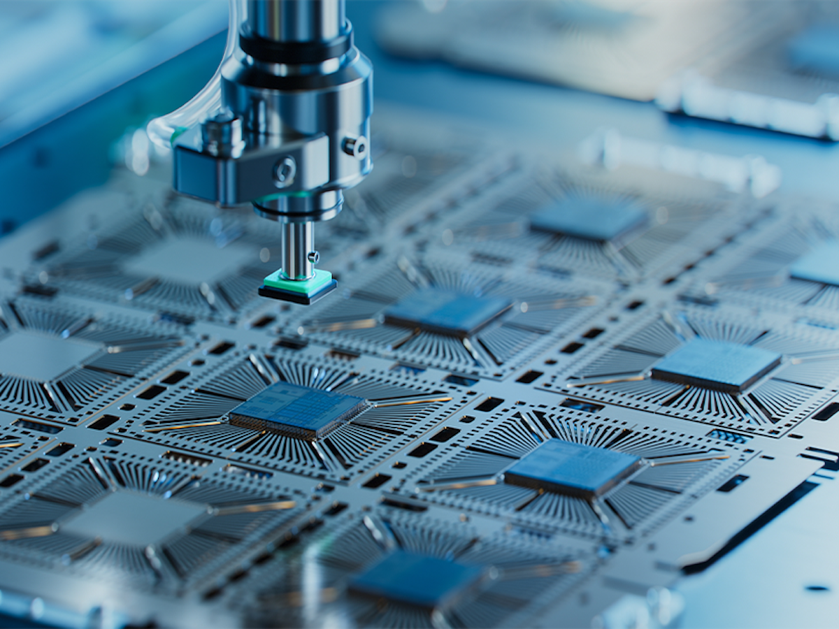
China is taking another step in memory-chip manufacturing
China’s semiconductor industry has reached another important manufacturing milestone.
ChangXin Memory Technologies (CXMT) says its fifth-generation DRAM technology platform, known as the G5 Platform, has entered mass production. The company announced the development on September 20 at the World Manufacturing Convention in Hefei, alongside two new LPDDR5X products.
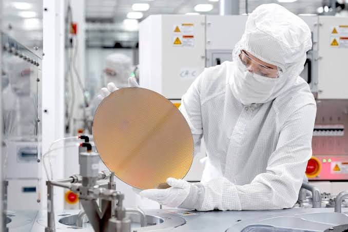
Why DRAM matters
DRAM is the short-term working memory used by smartphones, PCs, servers and many other electronic devices.
Unlike storage such as SSDs, DRAM needs to provide very fast access to data being actively processed.
That makes improvements in density, power efficiency and manufacturing cost particularly important.
The global DRAM market has long been dominated by Samsung, SK hynix and Micron. CXMT is trying to become a more significant fourth player.
11.95 nanometers and quadruple patterning
One of the headline specifications of the G5 announcement is 11.95 nanometers.
That figure refers to the company’s stated active-area half-pitch for the memory array. CXMT says it achieved this using quadruple patterning, a manufacturing approach that repeats patterning steps to create finer structures.
There is an important caveat, however.
An 11.95nm active-area half-pitch should not be treated as an 11.95nm logic-process node.
Memory manufacturers use different technical metrics to describe their processes, so directly comparing this number with node names used by Samsung, SK hynix or logic-chip manufacturers can create a misleading impression.
24Gb LPDDR5X for smartphones
The most commercially concrete part of the announcement is CXMT’s introduction of two 24Gb LPDDR5X products per die.
The company says this represents a 50% capacity increase over its previous comparable products. The two versions use 496-ball and 245-ball packages and target smartphones and other portable electronics. CXMT says both are already in mass production.
LPDDR is particularly important for mobile devices because power consumption matters heavily in smartphones and portable computers.
A larger pool of competitive suppliers could eventually affect:
- component costs;
- memory availability;
- smartphone design;
- memory capacity;
- supplier negotiations.
What does “50% more dies per wafer” actually mean?
CXMT says the G5 platform can produce at least 50% more gross dies per wafer than its previous generation, using a normalized 8Gb baseline.
But this should not be interpreted as an automatic 50% increase in sellable chips.
The semiconductor industry also cares about yield — the percentage of manufactured dies that pass the required tests and become usable products.
That means the more meaningful indicators over the coming months will be:
- actual wafer output;
- manufacturing yield;
- usable chip output;
- customer adoption;
- shipment volumes;
- production cost.

What does this mean for Samsung, SK hynix and Micron?
CXMT is entering a market where the established leaders already have enormous manufacturing experience and scale.
The announcement therefore does not by itself prove that the global DRAM hierarchy has changed.
What it does demonstrate is increasing competitive pressure.
If CXMT can maintain strong yields, produce at high volume and persuade smartphone and electronics manufacturers to adopt its products, the company could become a more important source of DRAM supply.
That could have consequences for pricing and supply-chain diversification.
The geopolitical dimension
The development also fits into China’s broader effort to reduce dependence on foreign semiconductor technologies.
Reuters linked the G5 milestone to China’s push to strengthen domestic semiconductor capabilities amid continuing U.S. restrictions on advanced chip technologies.
CXMT says the new platform was developed with domestic equipment makers involved in critical manufacturing processes and with extensive process simulation.
That matters because semiconductor independence is not simply about designing a chip.
It requires the ability to manufacture it repeatedly, at scale, with competitive yield and cost.
What G5 does not mean
It is also important not to confuse this announcement with the much more specialized HBM memory used in modern AI accelerators.
The current CXMT announcement focuses on DRAM and LPDDR5X, including products designed for smartphones and portable electronics.
So:
G5 is an important DRAM manufacturing milestone.
G5 is not evidence that China has solved advanced HBM manufacturing for AI accelerators.
What happens next?
The real test for CXMT now moves beyond the factory announcement.
The key questions are whether the new 24Gb LPDDR5X products appear in commercial devices, which manufacturers adopt them, how much volume CXMT can sustain and how competitive the final cost becomes.
If the chips move from mass production into high-volume consumer devices, the significance of the G5 platform will become much clearer.
Bottom line
CXMT has crossed another important threshold: a new DRAM manufacturing platform has moved from development into mass production.
The company’s figures — 11.95nm active-area half-pitch, at least 50% more gross dies per wafer and 24Gb LPDDR5X products — point to substantial efforts to improve memory density and manufacturing efficiency.
But the most important test is no longer the laboratory or factory announcement.
It is how many usable chips can actually be produced, how many customers adopt them, and how competitive CXMT becomes in the global market.
Editorial verification note: G5 specifications and the 24Gb product details come from CXMT’s official announcement; Reuters independently reported the mass-production milestone and market context. Actual yield, monthly production volume and customer adoption were not disclosed in the sources reviewed.