The race to build more advanced chips is already moving beyond today’s High NA EUV technology.
ASML and ZEISS have revealed details of Hyper NA, a potential next-generation EUV lithography system capable of printing features as small as 5 nanometers.
A peer-reviewed paper suggests such a system could be operational in roughly a decade, although ASML has not yet committed to commercial production.
What is Hyper NA?
Lithography uses light to transfer extremely small patterns onto silicon wafers.
ASML currently dominates the market for the most advanced EUV lithography systems.
Its High NA platform increased numerical aperture from 0.33 to 0.55, enabling smaller and more precise patterns.
Hyper NA aims to push that capability further.
The 5-nanometer target
The technical paper published in the Journal of Micro/Nanopatterning, Materials and Metrology says Hyper NA could print features as small as 5 nanometers.
Smaller structures can allow manufacturers to place more transistors into a given area and potentially improve performance and energy efficiency.
However, modern chip scaling increasingly relies on 3D architectures and advanced packaging as well.
Why ZEISS matters
ZEISS is ASML’s strategic optics partner.
Its mirrors are critical to EUV systems because EUV light cannot be handled with conventional lenses.
ZEISS says its High NA mirrors require extreme measurement precision at the subnanometer level.
According to the new paper, ZEISS can already produce mirrors precise enough for Hyper NA.
High NA is already entering production


While Hyper NA remains a future technology, High NA is already being used.
ASML and Intel said in September that High NA is being used in high-volume manufacturing at Intel Foundry for selected layers of Intel Core Ultra Series 3 processors. More than one million wafers had been processed across certification, R&D and production activities.
Samsung and SK Hynix plan to follow with High NA in 2028, while TSMC is targeting 2030.
KEY TAKEAWAYS
- ASML and ZEISS are developing the concept of Hyper NA, the next generation beyond High NA EUV lithography.
- The technology targets features as small as 5 nanometers.
- A peer-reviewed technical paper suggests the technology could be operational in roughly 10 years.
- Hyper NA would move beyond the 0.55 numerical aperture used by High NA.
- ZEISS says it already has capabilities relevant to the extremely precise mirrors required.
- ASML has begun development but has not committed to commercial production.
- The technology could become important for future AI chips because smaller features can support higher performance and energy efficiency.
Why AI needs better lithography

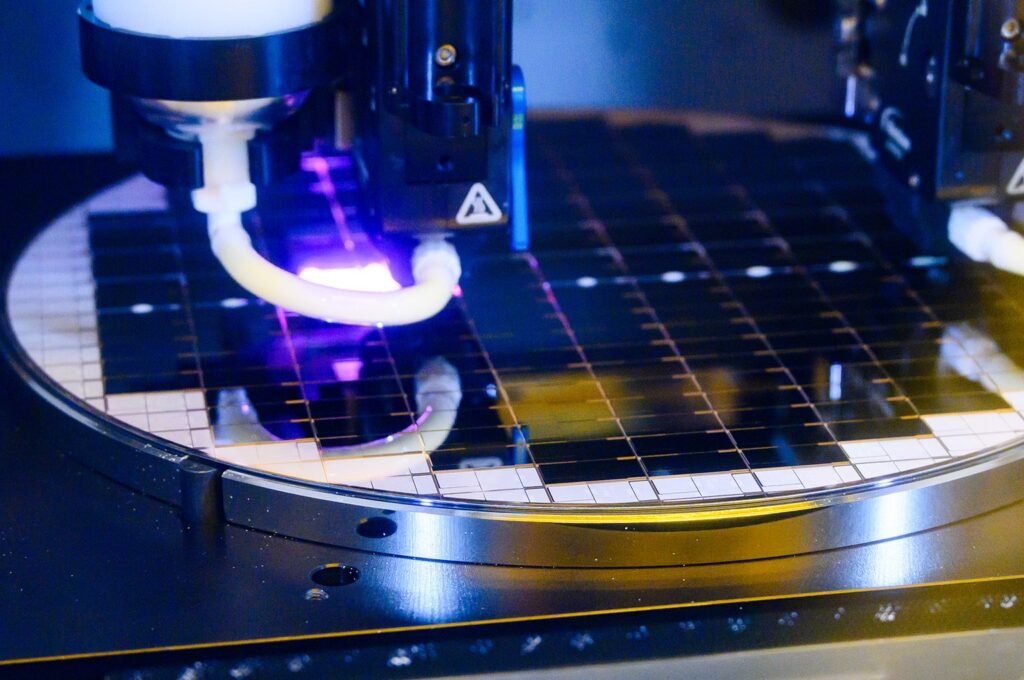
Modern AI accelerators depend on highly advanced semiconductor processes.
More efficient transistors can help improve computing performance while reducing energy consumption.
That matters enormously for AI data centers, where thousands of processors can operate simultaneously.
The impact of Hyper NA, if commercialized, could therefore extend to GPUs, servers, smartphones and future AI accelerators.
What comes after Hyper NA?
The technology may not be the final step.
The authors suggest that future lithography systems could eventually require even shorter wavelengths of light.
Research into free-electron lasers and X-ray lithography is already exploring possible alternatives.
Hyper NA is not a product coming to market tomorrow.
It is a long-term technology bet aimed at keeping semiconductor scaling alive into the next decade.
If ASML and ZEISS succeed in turning the concept into a production system, the technology could help enable denser, faster and more energy-efficient chips for AI and other demanding computing workloads.
The next AI breakthrough may therefore depend not only on better algorithms, but also on machines capable of drawing structures only a few nanometers wide.